|

Spreading Resistance Analysis (SRA) determines a resistivity-depth profile in silicon. Using published values of carrier mobility, a majority carrier concentration-depth
profile can be calculated. Going one step further, a dopant profile can be calculated by accounting for the space-charge redistribution under the bevel used for the spreading
resistance profile. Poisson's equation is solved iteratively, subject to boundary conditions consistent with the carrier concentration profile. We believe the results
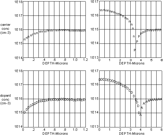
to be reasonable representations of the dopant distributions associated with the resistivity profiles we measured. We plot |NA-ND|, and used the symbol
"A" where the difference is positive, and "D" where it is negative. An excellent discussion of the implications here appears in the paper by Vandervorst
and Clarysse, Journal Electrochem. Soc. 137, 679 (1990). See also D. H. Dickey, J. Vac. Sci. Technol. B 10 (1), Jan/Feb 1992.
Two simple examples are shown below. On the left, the surface dopant concentration is revealed to be more seriously compensated than suggested by the carrier concentration
profile. The n-well profile at the right illustrates the discrepancy between electrical junction depth as measured on a bevel and true metallurgical junction depth.

|